GPIO Debugging Guide
The X3 chip has a total of 121 IO functional pins, each of which can be configured to work in GPIO mode. However, it is important to note the multiplexing relationship with other functional pins.
Pin Query
The multiplexing and configuration of IO pins can be found in the "PL-2500-3-X3 PIN SW Reg-V1.2.xls" and "RM-2500-5-X3M Register Reference Manual-GPIO&PIN-V1.1.pdf" in the datasheets.
In the "PL-2500-3-X3 PIN SW Reg-V1.2.xls", you can intuitively query the default power-on state, multiplexing, drive capability, pull-up/down, and Schmitt trigger configuration of each pin.
In the "RM-2500-5-X3M Register Reference Manual-GPIO&PIN-V1.1.pdf", you can find the GPIO register information for the corresponding pins.
Example
Taking the query of pin gpio120 as an example, we will explain the multiplexing, direction control, and data register address:
Functional multiplexing register description:
- Open the "PL-2500-3-X3 PIN SW Reg-V1.2.xls" and select the "PIN SW Register" data sheet.
- The first row will indicate the base address for functional multiplexing as
0xA6004000. - Find
GPIO[120]in theGPIOcolumn, and the corresponding information for this item is the default power-on state, multiplexing, drive capability, pull-up/down, and Schmitt trigger configuration of pin120. The image below shows the details.
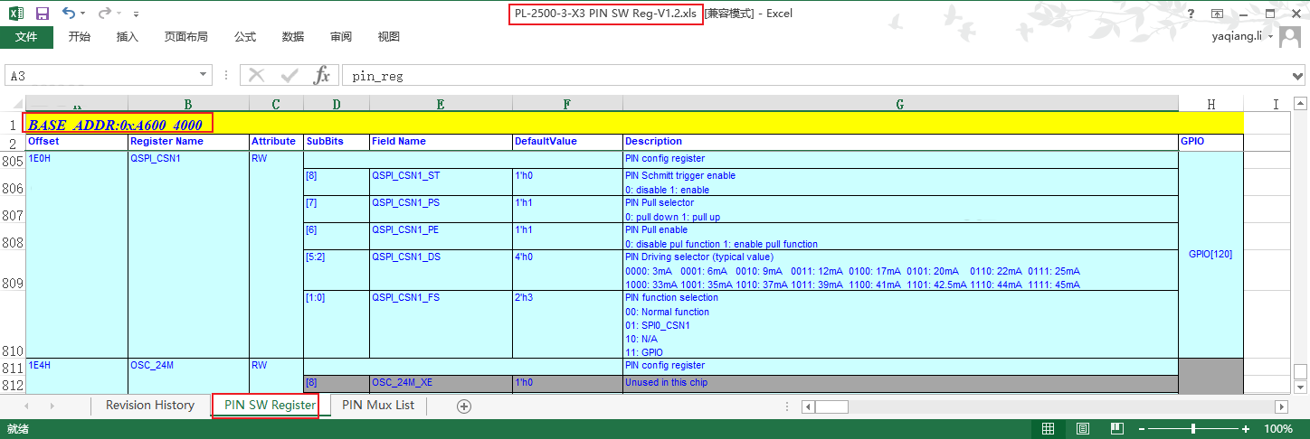
- After finding the above configuration items, adding the offset value to the base address will give the multiplexing control register of that pin. For example, the multiplexing register of
GPIO120is0xA6004000 + 0x1E0 = 0xA600410E0. - When configuring the multiplexing register, it is recommended to first read out the value, then set the corresponding bit you want to modify, and write it back. For example, to configure
GPIO120as aGPIOmode, only set the lower two bits of register0xA600410E0to0x3, while keeping other startup strength, pull-up/down, and Schmitt trigger configurations unchanged unless you explicitly know that you need to modify them as well.
GPIO control and data registers:
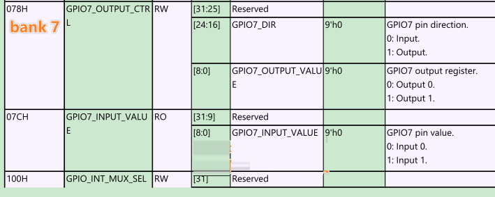
- Open the "RM-2500-5-X3M Register Reference Manual-GPIO&PIN-V1.1.pdf". This document has two main sections, the
GPIOsection describes the control registers, output data registers, input data registers, and pin voltage domain configuration registers (the two registers with offsets 0x170 and 0x174 are pin voltage domain configuration registers). The "Pin Group" section is the same as the multiplexing information in the "PL-2500-3-X3 PIN SW Reg-V1.2.xls" table. - The base address of the control and data registers is shown in the first row of each page table as
BASE_ADDR:0xA600_3000. Adding the queried offset address to this base address will give the corresponding complete register address. - The X3M chip has a total of 120 available pins, divided into 7 banks with a maximum of 16 pins per bank. The control and data registers are organized into one control unit per bank. For example, the bank of
GPIO120is7(obtained by dividing 120 by 16 and taking the integer part), and the pin number in the bank is8(obtained by taking the remainder of 120 divided by 16). With this information, we can find the corresponding register address as shown in the image below. The register ofGPIO120is thebit8in the registersGPIO7_xxx(counting from bit0).
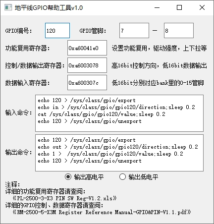
GPIO Helper Tool
With the information provided in the above sections, you should now have the ability to independently query and set the configurations of various pins. D-Robotics also provides a small software tool to help users quickly query the various register addresses of the pins and generate commands to assist in setting the pin functions. You can download and use the D-Robotics GPIO Helper Tool.
The interface of the tool is shown in the image below. Users can input the GPIO number or GPIO pin to query the various register addresses of the pin and generate helper commands for setting the pin. Please refer to the GPIO User Space Usage Guide for command details.
Driver Code
drivers/gpio/gpio-hobot-x3.c # gpio driver source file
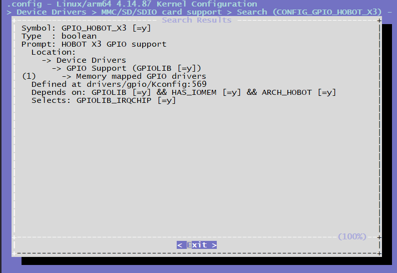
Kernel Configuration
CONFIG_GPIO_HOBOT_X3
Kernel DTS Configuration
/* arch/arm64/boot/dts/hobot/hobot-xj3.dtsi */
gpios: gpio@0xA6003000 {
    compatible = "hobot,x3-gpio";
    reg = <0 0xA6003000 0 0x100>;
    gpio-controller;
    #gpio-cells = <2>;
    gpio-ranges = <&pinctrl 0 0 121>;
    interrupts = <0 54 4>;
    interrupt-parent = <&gic>;
    interrupt-controller;
    #interrupt-cells = <2>;
};
The nodes in hobot-xj3.dtsi mainly declare some resources such as registers and interrupts, which are common features of the soc and are not related to specific circuit boards. Generally, there is no need to modify them.
Using GPIO
Kernel Space
DTS Configuration
The attributes of GPIO device tree nodes are generally named names-gpios or names-gpio, as shown below:
/* arch/arm64/boot/dts/hobot/hobot/hobot-x3-sdb.dtsi */
&usb_id {
        status = "okay";
        id-gpio = <&gpios 65 GPIO_ACTIVE_HIGH>;
        host-rst-gpio = <&gpios 115 GPIO_ACTIVE_HIGH>;
        host-exrst-gpio = <&gpios 38 GPIO_ACTIVE_LOW>;
};
Driver Code Interface
/* include/linux/gpio.h */
/* Request GPIO */
int gpio_request(unsigned gpio, const char *label);
/* Initialize GPIO as output and set output level */
int gpio_direction_output(unsigned gpio, int value);
/* Initialize GPIO as input */
int gpio_direction_input(unsigned gpio);
/* Get the level of GPIO */
int gpio_get_value(unsigned int gpio);
/* Set the level of GPIO */
void gpio_set_value(unsigned int gpio, int value);
/* Free GPIO */
void gpio_free(unsigned gpio);
/* Request GPIO interrupt and return the value that can be passed to request_irq and free_irq */
int gpio_to_irq(unsigned int gpio);
X3J3 GPIO IRQ
X3 GPIO has a total of 121 pins, and there are 4 hardware interrupts available. By setting the GPIO module registers, up to 4 pins out of the 121 pins can be mapped to the 4 IRQ interrupts. The mapping process is managed by the GPIO driver. The gpio_to_irq function is used to request GPIO IRQ numbers. If all 4 IRQs are already allocated, any subsequent requests will fail. The code for managing IRQ mapping is as follows:
/* drivers/gpio/gpio-hobot-x3.c */
/* Initialize the IRQ mapping table */
void init_irqbank(struct x3_gpio *gpo) {
    int i = 0;
    for (i = 0; i < GPIO_IRQ_BANK_NUM; i++) {
        gpo->irqbind[i] = GPIO_IRQ_NO_BIND;
    }
}

/* Request IRQ and update the mapping table */
int request_irqbank(struct x3_gpio *gpo, unsigned long gpio) {
    int i = 0, index = GPIO_IRQ_NO_BIND;
    index = find_irqbank(gpo, gpio);
    if(index == GPIO_IRQ_NO_BIND) {
        for (i = 0; i < GPIO_IRQ_BANK_NUM; i++) {
            if(gpo->irqbind[i] == GPIO_IRQ_NO_BIND) {
                gpo->irqbind[i] = gpio;
                index = i;
                break;
            }
        }
    } else {
        dev_err(gpo->dev, "gpio(%ld) has be binded\n", gpio);
        return GPIO_IRQ_NO_BIND;
    }
    return index;
```/* free gpio and update mapping table */
void release_irqbank(struct x3_gpio *gpo, unsigned long gpio) {
    int index = GPIO_IRQ_NO_BIND;
    index = find_irqbank(gpo, gpio);
    if(index != GPIO_IRQ_NO_BIND) {
        gpo->irqbind[index] = GPIO_IRQ_NO_BIND;
    }
}
X3 GPIO interfaces in the Kernel Space are standard Linux interfaces. For more usage examples, please refer to Documentation/gpio/consumer.txt.
User Space
Control interface
/sys/class/gpio/export # Userspace can request control of a gpio in the userspace by writing the gpio number, for example, echo 42 > export
/sys/class/gpio/unexport # Opposite of export
/sys/class/gpio/gpiochip0 # gpio controller
Invocation interface
After exporting the control of the gpio using export will result in the path /sys/class/gpio/gpio42/, and the following attributes:
- direction: indicates the direction of the GPIO port, reading as "in" or "out", writing "in" or "out" can set it as input or output
- value: indicates the level of the GPIO, 0 for low level, 1 for high level. If the GPIO is configured as output, the value can be written.
- edge: indicates the interrupt trigger mode, with 4 types: "none", "rising", "falling", and "both". "none" means the GPIO is not an interrupt pin, "rising" means the pin is triggered by a rising edge, "falling" means the pin is triggered by a falling edge, and "both" means the pin is triggered by an edge.
Invocation example
The example below demonstrates exporting the JTG_TRSTN pin, setting it as output, outputting a high level, and finally unexporting it.
echo 4 > /sys/class/gpio/export
echo out > /sys/class/gpio/gpio4/direction
echo 1 > /sys/class/gpio/gpio4/value
# echo 0 > /sys/class/gpio/gpio4/value
echo 4 > /sys/class/gpio/unexport
Debug interface
If the Linux Kernel configuration option CONFIG_DEBUG_FS is enabled and the debugfs file system is mounted
mount -t debugfs none /sys/kernel/debug
Then you can view the list of GPIO requests through the following node.
root@x3dvbx3-hynix1G-2666:~# cat /sys/kernel/debug/gpio
gpiochip0: GPIOs 0-120, parent: platform/a6003000.gpio:
gpio-42  (           |sysfs     ) in hi
gpio-64  (           |cd        ) in lo IRQ
gpio-65  (           |id        ) in hi IRQ
gpio-100 (           |?         ) out lo
gpio-120 (           |?         ) out hi
root@x3dvbx3-hynix1G-2666:~#
The X3 GPIO interface in User Space is a standard Linux interface. For more usage methods, please refer to Documentation/gpio/sysfs.txt.