RDK S100 40-pin UART and I2C
This handbook follows the recorded course slides, including wiring, commands, measured results, and the scope of verification.
Build two minimal links with loopback and a PCF8574T module.
Two buses, two evidence types
UART uses transmit-and-receive equality. I2C uses address discovery and data write-back.
UART2
Short Pins 8 and 10, then receive the same AA55 bytes.
I2C4
Connect Pins 27 and 28 to PCF8574T and detect address 0x20.
Minimal setup
No USB-to-TTL adapter, analyzer, or external power supply.
UART and I2C serve different links
UART
Point-to-point asynchronous communication over TX and RX.
I2C
Shared clock and data lines with address-based devices.
Logic level
Both S100 40-pin interfaces use 3.3 V logic.
Shared goal
Verify the full path from Linux device node to physical wiring.
Understand the SW6 selection
I2C5 and UART2 on J24 are selected by the 40 PIN switch. This lesson uses UART2, then keeps it selected while I2C runs on independent I2C4.
- Power off before moving SW6
- UART2 uses physical Pins 8 and 10
- I2C5 uses Pins 3 and 5
- I2C4 uses Pins 27 and 28
- I2C4 remains available while UART2 is selected
UART2 loopback wiring
Use one jumper to connect Pin 8 TXD directly to Pin 10 RXD. Do not connect power or ground for this loopback.
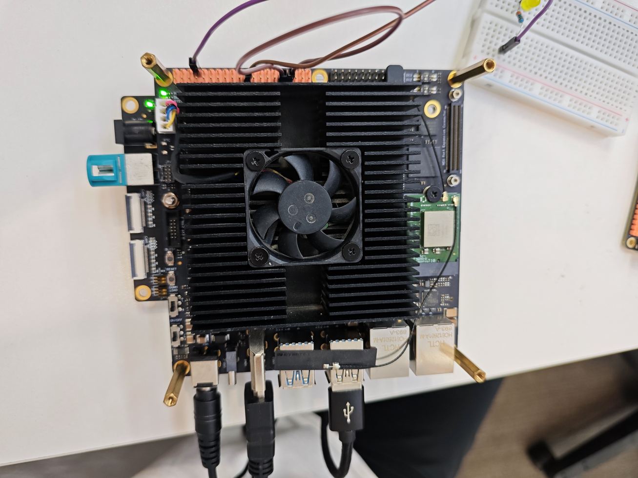
Pin 8 TXD ↔ Pin 10 RXD
Enable UART2 in hardware and software
UART2 is disabled by default. The verified setup keeps a recovery backup, enables uart2, and disables multiplexed i2c5.
Step 1
Power off and set the SW6 40 PIN switch to UART2.
Step 2
Set uart2 to okay and i2c5 to disabled in the device tree.
Step 3
Reboot and confirm that /dev/ttyS2 exists.
Step 4
Connect Pins 8 and 10, then start the loopback.
Send AA55 and verify the return
The measured run uses /dev/ttyS2 at 921600 baud. Transmitted and received bytes match exactly.
Device node
Confirm the node before testing.
Loopback result
Compare bytes, not only process startup.
UART loopback evidence
Open/dev/ttyS2
Configure921600 8N1
TransmitAA55
ReceiveAA55
AcceptByte match PASS
I2C4 avoids another SW6 change
I2C4 is available independently on Pins 27 and 28. The S100 provides 3.3 V power to the module.
Bus
/dev/i2c-4
Power
Pin 17 supplies 3.3 V and Pin 20 is ground.
Peripheral
The measured PCF8574T address is 0x20.
Four-wire PCF8574T connection
VCC, ground, SDA, and SCL are all required. The module uses 3.3 V power and 3.3 V logic.
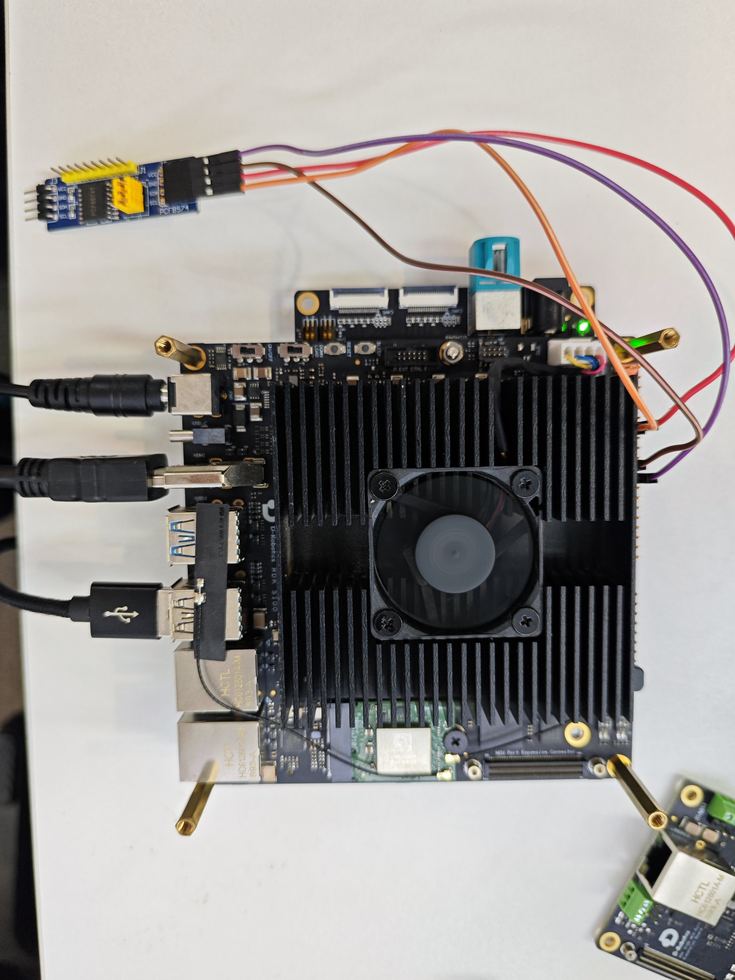
Pin 17→VCC | Pin 20→GND | Pin 27→SDA | Pin 28→SCL
Scan the address before reading
A0, A1, and A2 determine the module address, so discovery comes before any hard-coded value.
Scan the bus
This run finds 0x20; 0x2F is also present on the board.
Official sample
Choose i2c-4 and enter the detected address.
I2C read and write evidence
EnumerateFind /dev/i2c-4
ScanDetect 0x20
ReadReturn 0xFF
Write backSend a test value
AcceptRead/write PASS
Communication failure checks
Verify pin multiplexing and device nodes before changing the wiring.
UART
If ttyS2 is absent, check SW6, the device tree, and reboot.
Loop
If transmit works but receive is empty, inspect Pins 8 and 10.
I2C
If 0x20 is absent, inspect 3.3 V, ground, SDA, and SCL.
Address
Do not mistake the board device at 0x2F for PCF8574T.
complete
UART2 loopback and I2C4 peripheral access now have repeatable terminal evidence.
UART2 PASS
AA55 transmit and receive bytes match.
I2C4 PASS
0x20 is detected, read, and written back.
Next lesson
Verify SPI0 full-duplex loopback with one jumper.