GPIO Debugging Guide
The X5 chip has a total of 308 I/O pins, with 129 pins that can be configured to work in GPIO mode. However, it's important to be aware of the multiplexing relationships with other function pins.
Pin Query
You can query the multiplexing and configuration of I/O pins, including their default power-on states, multiplexing, drive capability, pull-up/pull-down, Schmitt trigger configuration, and corresponding GPIO register information in the datasheets under the file X5 PIN SW Reg-V1.1.xlsx (referred to as "the table" below).
Example
Here is an example of querying the multiplexing, direction control, and data register address for the pin LSIO_UART3_RXD:
Function Multiplexing Register Description:
-
Open the table and select the
PIN Mux Listsheet. -
Column B contains the
PinName, where you can find the row forLSIO_UART3_RXD. Column F shows the default function asLSIO_GPIO0_PIN10, which indicates the function is GPIO and the GPIO name isLSIO_GPIO0_PIN10. Columns I, K, M, and O describe the corresponding functions, as shown in the image below:
-
To configure the pin function, select the
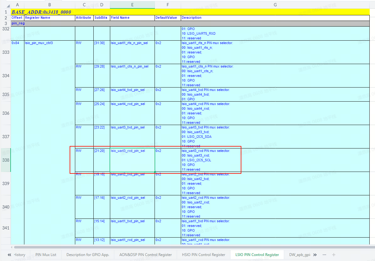
LSIO PIN Control Registersheet, as shown below:
- The first row of the table records the base address of the register, which is
0x34180000. - Column A records the offsets of various registers.
- Column G describes the functions of the registers.
- Find the row for "
lsio_uart3_rxd PIN mux selector" in column G to locate the register offset forLSIO_UART3_RXD's PIN mux register as0x84. The complete address can be calculated asBase Address + Offset = 0x34180000 + 0x84 = 0x34180084. - After finding the configuration item, you can set the corresponding PIN function. For example, writing
bit20-21 = 0x0in register0x34180084configuresLSIO_UART3_RXDasuart3 rx(Function 0). Writing0x1configures it asi2c5 scl(Function 1), and0x2configures it asGPIO(Function 2).
- The first row of the table records the base address of the register, which is
-
To configure the PIN attributes, select the
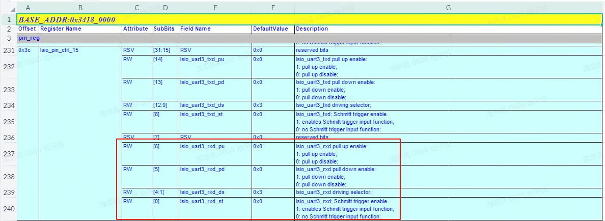
LSIO PIN Control Registersheet as shown below:
- The first row records the base address, which is
0x34180000. - Column A records the offsets of various registers.
- Column G describes the functions of the registers.
- Find the row for "
lsio_uart3_rxd pull up enable" in column G, which shows the register offset for PU/PD/Schmitt trigger control as0x3C. The complete address is0x34180000 + 0x3C = 0x3418003C. - PIN drive strength values can be found in the
Description for GPIO Apptable in the datasheet. - To find the power domain of the PIN, search for
mode selectand confirm that the corresponding register controls theLSIO_UART3_RXDpin. The register offset for controlling the power domain is0x38, and the complete address is0x34180000 + 0x38 = 0x34180038, as shown below:
- The first row records the base address, which is
-
When configuring registers, it is recommended to first read the current value, modify the necessary register bits, and then write it back.
GPIO Control and Data Registers:
-
The tables
DW_apb_gpio8_mem_map_v1.0andDW_apb_gpio32_mem_map_v1.0describe the GPIO direction registers and value registers for the pins, as shown in the image below (fromDW_apb_gpio32_mem_map_v1.0):
-
For example, the
LSIO_UART3_RXDpin corresponds to GPIOLSIO_GPIO0_PIN10. In the above image, the base address of theLSIO_GPIO0controller is0x34120000. Therefore, the data register address is0x34120000and the direction register address is0x34120004. The bit offset for the pinLSIO_UART3_RXDis 10, corresponding to GPIO numberLSIO_GPIO0_PIN10.
Driver Code
kernel/drivers/gpio/gpio-dwapb.c # gpio驱动源文件
Kernel Configuration
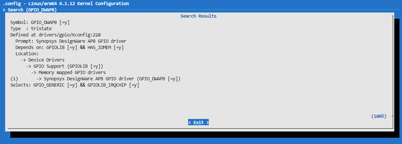
GPIO_DWAPB

Kernel DTS Configuration
The device tree definition for X5 GPIO controllers is located in the SDK package under the arch/arm64/boot/dts/hobot/x5.dtsi file.
The nodes in x5.dtsi mainly declare SoC-specific features and are not board-specific, so generally, they do not require modification.
GPIO Usage
Kernel Space
DTS Configuration
All GPIO configurations for X5 pins are located in the SDK package under the arch/arm64/boot/dts/hobot/pinmux-gpio.dtsi file.
If you need to configure specific pins for GPIO functionality, you can directly reference the predefined GPIO configurations.
/* arch/arm64/boot/dts/hobot/hobot/x5-som.dtsi */

&extcon_usb2otg {
	pinctrl-names = "default";
	pinctrl-0 = <&aon_gpio_6>;

	id-gpios = <&aon_gpio_porta 6 GPIO_ACTIVE_HIGH>;

	status = "okay";
};
Driver Code Interface
/* include/linux/gpio.h */
/* Request GPIO */
int gpio_request(unsigned gpio, const char *label);
/* Initialize GPIO as output and set output level */
int gpio_direction_output(unsigned gpio, int value);
/* Initialize GPIO as input */
int gpio_direction_input(unsigned gpio);
/* Get the value of the GPIO pin */
int gpio_get_value(unsigned int gpio);
/* Set the value of the GPIO pin */
void gpio_set_value(unsigned int gpio, int value);
/* Release the GPIO pin */
void gpio_free(unsigned gpio);
/* Request a GPIO interrupt; the returned value can be passed to request_irq and free_irq */
int gpio_to_irq(unsigned int gpio);
X5 GPIO IRQ
The X5 chip has a total of 129 GPIO pins, all of which can be configured for interrupt functionality.
The X5 GPIO controller supports interrupt triggers on rising edge, falling edge, high level, or low level. Each GPIO configured as an interrupt can have its trigger condition independently set.
X5 GPIO interfaces in Kernel Space adhere to standard Linux interfaces. For more details on usage, refer to Documentation/driver-api/gpio/consumer.rst.
User Space
Control Interface
Note: In the Linux-V6.1 baseline used by X5, the GPIO sysfs interface has been marked as "Obsolete." For more details, refer to the Linux documentation.
/sys/class/gpio/export  # The user space can export the control of a GPIO to the user space by writing the GPIO number to this file, e.g., `echo 356 > export`
/sys/class/gpio/unexport  # The opposite of `export`, used to unexport a GPIO from user space
/sys/class/gpio/gpiochip0  # GPIO controller
API Usage
After exporting the GPIO control using export, a path like /sys/class/gpio/gpio356/ will be created. This path contains the following attributes:
- direction: Specifies the GPIO port direction. It can be read as "in" or "out", and written as either "in" or "out" to set it as input or output.
- value: Represents the GPIO level. 0 indicates low level, and 1 indicates high level. If the GPIO is configured as an output, the
valuecan be written to change the state. - edge: Specifies the interrupt trigger type. It can have one of four values: "none", "rising", "falling", or "both".
- "none" means the GPIO is not an interrupt pin.
- "rising" means the pin triggers an interrupt on the rising edge.
- "falling" means the pin triggers an interrupt on the falling edge.
- "both" means the pin triggers an interrupt on either edge.
Example Usage
The following example demonstrates exporting the LSIO_UART3_RXD pin, setting it to output mode, outputting a high level, and then unexporting it.
echo 356 > /sys/class/gpio/export
echo out > /sys/class/gpio/gpio356/direction
echo 1 > /sys/class/gpio/gpio356/value
# echo 0 > /sys/class/gpio/gpio356/value
echo 356 > /sys/class/gpio/unexport
Debugging Interface
If the CONFIG_DEBUG_FS option is enabled in the kernel configuration and the debugfs filesystem is mounted, the kernel provides a GPIO debugging interface via debugfs.
First, check whether debugfs is mounted. If the following command outputs anything, it indicates that debugfs is currently mounted:
mount | grep debugfs
If the output is empty, execute the following command to mount debugfs:
mount -t debugfs none /sys/kernel/debug
Once debugfs is successfully mounted, you can view the list of GPIO allocations through the following node:
# cat /sys/kernel/debug/gpio
gpiochip9: GPIOs 347-378, parent: platform/34130000.gpio, 34130000.gpio:
 gpio-352 (                    |enable              ) out lo

gpiochip8: GPIOs 379-410, parent: platform/34120000.gpio, 34120000.gpio:
 gpio-410 (                    |phyreset            ) out hi

gpiochip7: GPIOs 411-433, parent: platform/32150000.gpio, 32150000.gpio:

gpiochip6: GPIOs 434-465, parent: platform/35070000.gpio, 35070000.gpio:
 gpio-435 (                    |voltage             ) out hi ACTIVE LOW

gpiochip5: GPIOs 466-497, parent: platform/35060000.gpio, 35060000.gpio:
 gpio-492 (                    |power               ) out hi

gpiochip4: GPIOs 498-505, parent: platform/31000000.gpio, 31000000.gpio:
 gpio-500 (                    |GPIO Key Power      ) in  hi IRQ ACTIVE LOW
 gpio-503 (                    |id                  ) in  hi IRQ
 gpio-504 (                    |id                  ) in  hi IRQ

gpiochip3: GPIOs 506-507, parent: platform/34180000.lsio_iomuxc, 34180000.lsio_iomuxc:

gpiochip2: GPIOs 508-508, parent: platform/31040014.dsp_iomuxc, 31040014.dsp_iomuxc:

gpiochip1: GPIOs 509-510, parent: platform/35050000.hsio_iomuxc, 35050000.hsio_iomuxc:

gpiochip0: GPIOs 511-511, parent: platform/31040000.aon_iomuxc, 31040000.aon_iomuxc:
#
The output above is just an example; the actual output depends on the board's specific DTS configuration.
X5 GPIOs in User Space follow the standard Linux GPIO interfaces. For more usage methods, refer to Documentation/gpio/sysfs.txt.
Linux GPIO Number to Chip Pin Mapping
Note: The GPIO numbers in Linux are purely a software concept and may change depending on software configurations. There is no physical binding between the GPIO numbers and the chip's pin numbers.
It is recommended to use the hb_gpioinfo tool to check the mapping of PinName, PinNum, and PinFunc on the current development board.
If the hb_gpioinfo tool is not available on the board, you can update hobot-io via apt.
hb_gpioinfo Usage Example:
- PinName: Refers to the pin name on the SoC, which is consistent with the pin naming in the X5 SoC schematic.
- PinNum: Refers to the actual GPIO number corresponding to the X5 chip's pin.
- PinFunc: Refers to the pin's multiplexing function that has been used in the X5 device tree. When checking
PinFunc, note that if it showsDefault, it means that the device tree has not assigned that function to the pin. In this case, you should check what the default functionality of the pin is in the pinlist.
gpiochip0 - 8 lines: @31000000.gpio: @498-505
[Number] [Mode] [Status] [GpioName] [PinName] [PinNum] [PinFunc]
line 0: unnamed input AON_GPIO_PIN0 498 Default
line 1: unnamed input AON_GPIO_PIN1 499 Default
line 2: unnamed input active-low GPIO Key Power AON_GPIO_PIN2 500 aon_gpio_2
line 3: unnamed input interrupt AON_GPIO_PIN3 501 Default
line 4: unnamed input AON_GPIO_PIN4 502 Default
line 5: unnamed input id AON_ENV_VDD 503 aon_gpio_5
line 6: unnamed input id AON_ENV_CNN0 504 aon_gpio_6
line 7: unnamed input AON_ENV_CNN1 505 aon_gpio_7
gpiochip1 - 31 lines: @35060000.gpio: @466-496
[Number] [Mode] [Status] [GpioName] [PinName] [PinNum] [PinFunc]
line 0: unnamed input HSIO_ENET_MDC 466 enetgrp
line 1: unnamed input HSIO_ENET_MDIO 467 enetgrp
line 2: unnamed input HSIO_ENET_TXD_0 468 enetgrp
line 3: unnamed input HSIO_ENET_TXD_1 469 enetgrp
line 4: unnamed input HSIO_ENET_TXD_2 470 enetgrp
line 5: unnamed input HSIO_ENET_TXD_3 471 enetgrp
line 6: unnamed input HSIO_ENET_TXEN 472 enetgrp
line 7: unnamed input HSIO_ENET_TX_CLK 473 enetgrp
line 8: unnamed input HSIO_ENET_RX_CLK 474 enetgrp
line 9: unnamed input HSIO_ENET_RXD_0 475 enetgrp
line 10: unnamed input HSIO_ENET_RXD_1 476 enetgrp
line 11: unnamed input HSIO_ENET_RXD_2 477 enetgrp
line 12: unnamed input HSIO_ENET_RXD_3 478 enetgrp
line 13: unnamed input HSIO_ENET_RXDV 479 enetgrp
line 14: unnamed input HSIO_ENET_PHY_CLK 480 enetgrp
line 15: unnamed input HSIO_SD_WP 481 sdgrp
line 16: unnamed input HSIO_SD_XLK 482 sdgrp
line 17: unnamed input HSIO_SD_CMD 483 sdgrp
line 18: unnamed input HSIO_SD_CDN 484 sdgrp
line 19: unnamed input HSIO_SD_DATA0 485 sdgrp
line 20: unnamed input HSIO_SD_DATA1 486 sdgrp
line 21: unnamed input HSIO_SD_DATA2 487 sdgrp
line 22: unnamed input HSIO_SD_DATA3 488 sdgrp
line 23: unnamed output phyreset HSIO_SDIO_WP 489 hsio_gpio0_23
line 24: unnamed input HSIO_SDIO_XLK 490 sdiogrp
line 25: unnamed input HSIO_SDIO_CMD 491 sdiogrp
line 26: unnamed output power HSIO_SDIO_CDN 492 hsio_gpio0_26
line 27: unnamed input HSIO_SDIO_DATA0 493 sdiogrp
line 28: unnamed input HSIO_SDIO_DATA1 494 sdiogrp
line 29: unnamed input HSIO_SDIO_DATA2 495 sdiogrp
line 30: unnamed input HSIO_SDIO_DATA3 496 sdiogrp
gpiochip2 - 18 lines: @35070000.gpio: @434-451
[Number] [Mode] [Status] [GpioName] [PinName] [PinNum] [PinFunc]
line 0: unnamed input HSIO_QSPI_SSN0 434 qspigrp
line 1: unnamed output active-low voltage HSIO_QSPI_SSN1 435 hsio_gpio1_1
line 2: unnamed input HSIO_QSPI_SCLK 436 qspigrp
line 3: unnamed input HSIO_QSPI_DATA0 437 qspigrp
line 4: unnamed input HSIO_QSPI_DATA1 438 qspigrp
line 5: unnamed input HSIO_QSPI_DATA2 439 qspigrp
line 6: unnamed input HSIO_QSPI_DATA3 440 qspigrp
line 7: unnamed input HSIO_EMMC_CLK 441 Default
line 8: unnamed input HSIO_EMMC_CMD 442 Default
line 9: unnamed input HSIO_EMMC_DATA0 443 Default
line 10: unnamed input HSIO_EMMC_DATA1 444 Default
line 11: unnamed input HSIO_EMMC_DATA2 445 Default
line 12: unnamed input HSIO_EMMC_DATA3 446 Default
line 13: unnamed input HSIO_EMMC_DATA4 447 Default
line 14: unnamed input HSIO_EMMC_DATA5 448 Default
line 15: unnamed input HSIO_EMMC_DATA6 449 Default
line 16: unnamed input HSIO_EMMC_DATA7 450 Default
line 17: unnamed input HSIO_EMMC_RSTN 451 Default
gpiochip3 - 23 lines: @32150000.gpio: @411-433
[Number] [Mode] [Status] [GpioName] [PinName] [PinNum] [PinFunc]
line 0: unnamed input DSP_I2C7_SCL 411 dsp_i2c7grp
line 1: unnamed input DSP_I2C7_SDA 412 dsp_i2c7grp
line 2: unnamed input DSP_UART0_RXD 413 uart0grp
line 3: unnamed input DSP_UART0_TXD 414 uart0grp
line 4: unnamed input DSP_I2S0_MCLK 415 i2s0grp
line 5: unnamed input DSP_I2S0_SCLK 416 i2s0grp
line 6: unnamed input DSP_I2S0_WS 417 i2s0grp
line 7: unnamed input DSP_I2S0_DI 418 i2s0grp
line 8: unnamed input DSP_I2S0_DO 419 i2s0grp
line 9: unnamed input DSP_I2S1_MCLK 420 Default
line 10: unnamed input DSP_I2S1_SCLK 421 Default
line 11: unnamed input DSP_I2S1_WS 422 Default
line 12: unnamed input DSP_I2S1_DI 423 Default
line 13: unnamed input DSP_I2S1_DO 424 Default
line 14: unnamed output active-low ACT DSP_PDM_CKO 425 32150000.gpio:425
line 15: unnamed input DSP_PDM_IN0 426 dsp_gpio0_15
line 16: unnamed input DSP_PDM_IN1 427 dsp_gpio0_16
line 17: unnamed output DSP_PDM_IN2 428 dsp_gpio0_17
line 18: unnamed output DSP_PDM_IN3 429 dsp_gpio0_18
line 19: unnamed input interrupt DSP_SPI6P_SCLK 430 dsp_gpio0_19
line 20: unnamed output active-low reset DSP_SPI6_SSN 431 dsp_gpio0_20
line 21: unnamed input interrupt DSP_SPI6_MISO 432 Default
line 22: unnamed input DSP_SPI6_MOSI 433 Default
gpiochip4 - 32 lines: @34120000.gpio: @379-410
[Number] [Mode] [Status] [GpioName] [PinName] [PinNum] [PinFunc]
line 0: unnamed input LSIO_UART7_RX 379 Default
line 1: unnamed input LSIO_UART7_TX 380 Default
line 2: unnamed input LSIO_UART7_CTS 381 Default
line 3: unnamed input LSIO_UART7_RTS 382 Default
line 4: unnamed input LSIO_UART1_RX 383 uart1grp
line 5: unnamed input LSIO_UART1_TX 384 uart1grp
line 6: unnamed output LSIO_UART1_CTS 385 lsio_gpio0_6
line 7: unnamed output reset LSIO_UART1_RTS 386 lsio_gpio0_7
line 8: unnamed input LSIO_UART2_RX 387 Default
line 9: unnamed input LSIO_UART2_TX 388 Default
line 10: unnamed input LSIO_UART3_RX 389 i2c5grp
line 11: unnamed input LSIO_UART3_TX 390 i2c5grp
line 12: unnamed input LSIO_UART4_RX 391 lsio_gpio0_12
line 13: unnamed output LSIO_UART4_TX 392 lsio_gpio0_13_rdk_v1p0
line 14: unnamed input LSIO_SPI0_SCLK 393 Default
line 15: unnamed input LSIO_SPI1_SSN_1 394 spi1_ssn1grp
line 16: unnamed input LSIO_SPI1_SCLK 395 spi1grp
line 17: unnamed input LSIO_SPI1_SSN 396 spi1grp
line 18: unnamed input LSIO_SPI1_MISO 397 spi1grp
line 19: unnamed input LSIO_SPI1_MOSI 398 spi1grp
line 20: unnamed input LSIO_SPI2_SCLK 399 Default
line 21: unnamed input LSIO_SPI2_SSN 400 Default
line 22: unnamed input LSIO_SPI2_MISO 401 Default
line 23: unnamed input LSIO_SPI2_MOSI 402 Default
line 24: unnamed input LSIO_SPI3_SCLK 403 pinctrl_lpwm1_0
line 25: unnamed input LSIO_SPI3_SSN 404 pinctrl_lpwm1_1
line 26: unnamed input LSIO_SPI3_MISO 405 Default
line 27: unnamed input LSIO_SPI3_MOSI 406 Default
line 28: unnamed input LSIO_SPI4_SCLK 407 uart5grp
line 29: unnamed input LSIO_SPI4_SSN 408 uart5grp
line 30: unnamed input LSIO_SPI4_MISO 409 i2c6grp
line 31: unnamed input LSIO_SPI4_MOSI 410 i2c6grp
gpiochip5 - 17 lines: @34130000.gpio: @347-363
[Number] [Mode] [Status] [GpioName] [PinName] [PinNum] [PinFunc]
line 0: unnamed input LSIO_SPI5_SCLK 347 spi5grp
line 1: unnamed input LSIO_SPI5_SSN 348 spi5grp
line 2: unnamed input LSIO_SPI5_MISO 349 spi5grp
line 3: unnamed input LSIO_SPI5_MOSI 350 spi5grp
line 4: unnamed input LSIO_SPI0_SSN 351 lsio_gpio1_4
line 5: unnamed output enable LSIO_SPI0_MISO 352 lsio_gpio1_5
line 6: unnamed input LSIO_SPI0_MOSI 353 lsio_gpio1_6
line 7: unnamed input LSIO_I2C0_SCL 354 i2c0grp
line 8: unnamed input LSIO_I2C0_SDA 355 i2c0grp
line 9: unnamed input LSIO_I2C1_SCL 356 pinctrl_pwm3_0
line 10: unnamed input LSIO_I2C1_SDA 357 pinctrl_pwm3_1
line 11: unnamed input LSIO_I2C2_SCL 358 i2c2grp
line 12: unnamed input LSIO_I2C2_SDA 359 i2c2grp
line 13: unnamed input LSIO_I2C3_SCL 360 i2c3grp
line 14: unnamed input LSIO_I2C3_SDA 361 i2c3grp
line 15: unnamed input LSIO_I2C4_SCL 362 i2c4grp
line 16: unnamed input LSIO_I2C4_SDA 363 i2c4grp